HomeProductsAboutCasesBlogContactGet Quote

Semiconductor Graphite Tooling

High-purity graphite components for wafer processing, crystal growth, epitaxy, and packaging.

Overview

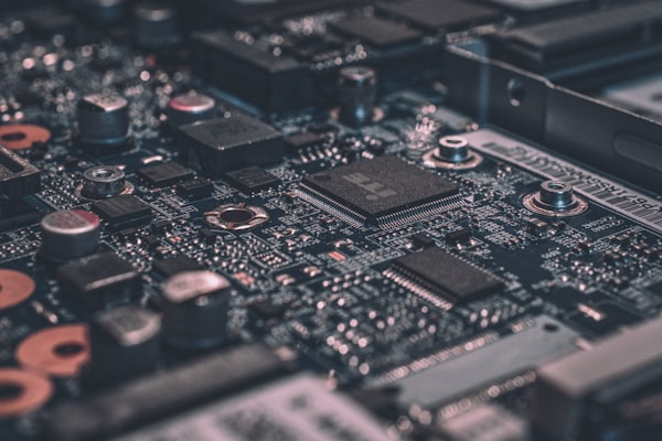
Baotan Graphite produces semiconductor-grade graphite tooling with ash content below 5ppm. Our components are used in MOCVD, SiC crystal growth, wafer processing, and advanced packaging — where purity, dimensional stability, and thermal performance are non-negotiable.

Three proprietary coating technologies ensure particle-free operation in the most demanding semiconductor environments.

Request Quote →
Semiconductor Tooling

Coating Technologies

Non-Shedding Coating

Eliminates particle generation in cleanrooms. Ideal for wafer handling and processing where contamination is critical.

Carbon Coating (4N–6N)

High-purity carbon coating achieving 99.99% to 99.9999%. Enhances conductivity, provides uniform non-reactive surface.

Nano-Hardening Coating

Increases surface hardness for wear-prone applications. Extends component life over thousands of cycles.

Product Range

CategoryComponentsApplication
Wafer ProcessingBoats, cassettes, susceptors, traysMOCVD, LPCVD, epitaxy, annealing
Crystal GrowthCrucibles, heaters, insulation, supportsSiC crystal growth (PVT), silicon pulling
SinteringBoats, trays, moldsMLCC, rare earth, Li-battery materials
PackagingEncapsulation fixtures, bonding toolsAdvanced semiconductor packaging
CustomAny custom-machined componentPer drawing — full OEM customization

Specifications

ParameterValue
MaterialIsostatic graphite (IG-110, EK3200 equivalents)
Ash Content≤ 5 ppm (std) / ≤ 2 ppm (ultra-high purity)
Density1.78 – 1.85 g/cm³
Grain Size5 – 10 µm
CoatingSiC (CVD) / Carbon / Nano-hardening / Non-shedding
CleanroomClass 1000 packaging available

Need Semiconductor Graphite Tooling?

Send specifications. Quote within 24 hours.

Get a Quote →